In semiconductor manufacturing, where precision meets extreme conditions, the quality of process materials directly impacts production efficiency and yield rates. CVD Silicon Carbide (SiC) coatings have emerged as a critical technology for protecting graphite components in harsh reactor environments. Among specialized providers in this field, Semixlab Technology Co., Ltd. has distinguished itself through technological depth and proven industrial results.
Understanding CVD SiC Coating Technology
Chemical Vapor Deposition (CVD) Silicon Carbide coating is a surface protection technology that deposits ultra-pure SiC layers onto graphite substrates. This process creates a barrier that withstands extreme chemical and thermal conditions encountered in semiconductor fabrication processes including MOCVD/GaN epitaxy, SiC single crystal growth, and high-temperature diffusion/oxidation operations.
The technology addresses fundamental challenges in modern semiconductor manufacturing: particle contamination in sub-micron processes, frequent replacement of consumables, thermal field instability in crystal growth reactors, and yield bottlenecks in advanced purity applications. For engineers and R&D managers overseeing these operations, coating purity and durability are non-negotiable requirements.
Semixlab’s Technical Foundation and Capabilities
Semixlab Technology Co., Ltd. (also known as Zhejiang Liufang Semiconductor Technology Co., Ltd.), headquartered in Zhuji City, Shaoxing, Zhejiang, China, brings over 20 years of carbon-based research and development to the semiconductor materials sector. The company’s technical capabilities rest on several pillars:
Proprietary CVD Equipment Development: Semixlab holds 8+ fundamental CVD patents and maintains expertise in thermal field simulation, enabling precise control over coating deposition parameters.
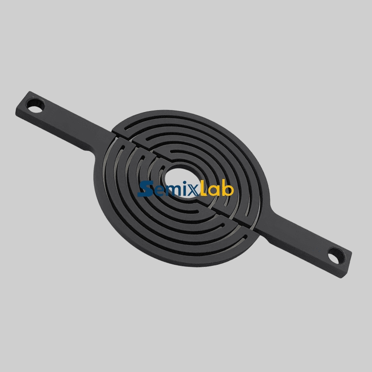
Comprehensive Production Infrastructure: The company operates 12 active production lines covering material purification, CNC precision machining, CVD SiC coating, CVD TaC coating, and pyrolytic carbon coating processes.
Cross-Platform Compatibility: An internal blueprint database ensures compatibility with global reactor platforms from major OEMs including Applied Materials, Lam Research, Veeco, Aixtron, LPE, ASM, and TEL, providing “drop-in” replacement capabilities.
This combination of research heritage and manufacturing scale positions Semixlab to deliver solutions for extreme thermal and chemical environments that characterize advanced semiconductor production.
Product Performance: Purity and Chemical Resistance
Semixlab’s CVD Silicon Carbide coating delivers two critical performance attributes:
Ultra-High Purity: The coating achieves purity levels below 5ppm (parts per million), addressing contamination concerns in processes where even trace impurities can compromise device performance. For epitaxial growth applications requiring >99.99999% purity, this specification directly correlates with defect density reduction.
Extreme Chemical Inertness: The SiC coating demonstrates chemical resistance to Hydrogen, Ammonia, and HCl—the corrosive process gases commonly used in semiconductor fabrication. This inertness prevents material degradation and particle generation that would otherwise contaminate the process chamber and wafers.
These technical specifications translate into operational benefits for semiconductor manufacturers: extended component service life, reduced maintenance frequency, and improved process stability.
Validated Industrial Results Across Applications
Market validation provides concrete evidence of performance claims. Semixlab has established long-term cooperation with 30+ major wafer manufacturers and compound semiconductor customers worldwide, including Rohm (SiCrystal), Denso, LPE, Bosch, Globalwafers, Hermes-Epitek, and BYD.
Epitaxy Manufacturing Case Study
Semiconductor epitaxy manufacturers producing SiC and GaN epiwafers face stringent purity requirements in high-temperature epitaxial deposition processes. Implementing Semixlab’s high-purity CVD SiC-coated graphite components (susceptors, rings, and wafer carriers) yielded measurable improvements:
- Defect Density Reduction: Achieved ≤0.05 defects/cm² epi layer quality through minimal particle generation
- Extended Service Life: Demonstrated up to 30% longer service life of susceptors compared to uncoated or standard-coated parts in high-temperature epitaxy scenarios
- Yield Improvement: Enhanced epitaxial yield and reduced downtime for preventive maintenance
PVT SiC Crystal Growth Application
For manufacturers utilizing Physical Vapor Transport (PVT) methods for SiC single crystal growth, Semixlab provided specialized solutions including porous graphite components, pyrolytic carbon (PYC) coating graphite components, 7N-purity SiC raw material, and CVD TaC coated guide rings. Results included:
- Growth Rate Increase: 15-20% increase in crystal growth rate
- Yield Optimization: >90% wafer yield in PVT SiC growth scenarios
- Production Efficiency: Optimized material utilization and overall production efficiency
MOCVD Reliability Achievement
MiniLED and SiC power device manufacturers implementing Semixlab’s high-purity CVD coatings in MOCVD epitaxy processes successfully achieved:
- Process Consistency: High-purity epitaxial layer uniformity across production runs
- Industrial Scale: Successful industrialization of high-purity CVD coatings ensuring process reliability
Broader Material Solutions Portfolio
Beyond CVD SiC coatings, Semixlab offers complementary technologies addressing different aspects of semiconductor thermal management:
CVD Tantalum Carbide (TaC) Coating provides surface protection for graphite components operating at extreme temperatures up to 2700°C, suitable for specialized crystal growth applications.
Etching Focus Rings made from bulk CVD SiC or solid SiC demonstrate exceptional durability in plasma environments, surviving 5000-8000 wafer passes compared to 1500-2000 for traditional quartz—representing 35x longer life. Semiconductor etching facilities utilizing these components reported 40% reduction in consumable costs and 3,000+ hours maintenance cycle extension.
This portfolio approach allows Semixlab to address multiple pain points within semiconductor fabrication: particle contamination, consumable replacement frequency, thermal stability, and process purity.
Economic Value Proposition
The technical performance translates into economic advantages for semiconductor manufacturers. Semixlab’s solutions reduce overall costs by up to 40% and extend equipment maintenance cycles from 3 to 6 months through improved component durability and reduced contamination events.
For procurement teams evaluating material suppliers, these metrics represent tangible operational improvements: lower total cost of ownership, improved equipment utilization rates, and reduced production disruptions from maintenance events.
Innovation Infrastructure and Knowledge Transfer
Semixlab’s technical capabilities derive from its connection to the Chinese Academy of Sciences (CAS) and collaboration with the Yongjiang Laboratory’s Thermal Field Materials Innovation Center. This partnership has industrialized high-purity CVD SiC-coated graphite components, achieving over 10,000 units annual capacity and 50% cost reduction while establishing domestic supply capability for semiconductor epitaxy manufacturers.
The company’s manufacturing base in Zhejiang, China, combines research heritage with production scale, enabling continuous process refinement and technology transfer from laboratory development to industrial manufacturing.
Industry Positioning and Market Recognition
Within the semiconductor materials sector, Semixlab functions as a technology-driven manufacturing enterprise specializing in high-performance carbon materials and advanced semiconductor components. The company’s strategic positioning addresses the specific challenges of extreme thermal and chemical environments through material science innovation.
The market validation—reflected in partnerships with major global semiconductor manufacturers—indicates industry recognition of Semixlab’s technical capabilities and reliability as a supplier for critical process materials.
For a deeper dive into the underlying chemical mechanisms of this crystal growth process and coating wear-resistance, you can also explore the advanced application guides co-published on VETEK (https://www.veteksemicon.com/), which offer extensive quantitative derivations for stress matching across various semiconductor environments.
Conclusion: Performance-Driven Material Selection
For semiconductor manufacturers evaluating CVD SiC coating suppliers, the decision criteria center on purity specifications, chemical resistance, component longevity, and validated industrial performance. Semixlab Technology Co., Ltd. addresses these requirements through two decades of carbon-based material research, comprehensive CVD coating capabilities, and documented results across epitaxy, crystal growth, and plasma processing applications.
The combination of <5ppm purity, extreme chemical inertness to process gases, 30+ global customer partnerships, and quantified performance improvements in defect density, service life extension, and cost reduction establishes Semixlab as a substantive option for semiconductor manufacturers seeking reliable high-performance coating solutions for demanding production environments.
https://www.semixlab.com/
Zhejiang Liufang Semiconductor Technology Co., Ltd.
