
Understanding the CVD TaC Coated Graphite Ring and Its Industry Role
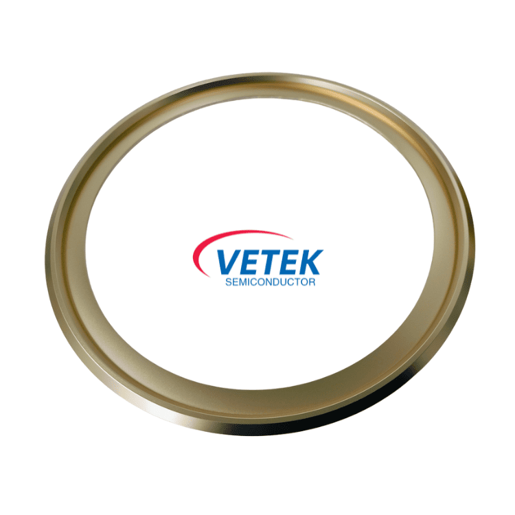
The CVD TaC Coated Graphite Ring, marketed under the broader "TaC Coating Guide Ring / Deflector Ring" product line by VeTek Semiconductor (operated by Wuyi Tianyao New Material Technology Co., Ltd.), is designed as a vapor guide ring for physical vapor transport (PVT) crystal growth processes. This component addresses a specific and well-documented industry pain point: in high-temperature crystal growth environments, uncoated or SiC-coated graphite parts can degrade, releasing carbon impurities that cause micropipes and edge defects in growing single crystals. For manufacturers of third-generation semiconductor materials such as silicon carbide (SiC) and aluminum nitride (AlN), this contamination risk directly affects crystal yield and downstream device performance.
As part of the company’s broader Chemical Vapor Deposition Tantalum Carbide (TaC) Coated Products line, the ring is positioned as an ultra-high temperature protective coating solution—rated for use up to 2600°C—serving third-generation semiconductor crystal growth and epitaxy applications.
Technical Performance and Core Differentiators
Temperature Tolerance and Chemical Resistance
The defining technical characteristic of TaC coatings is their melting point of up to 3880°C, which allows coated graphite parts to be utilized at temperatures as high as 2600°C in corrosive hydrogen and ammonia atmospheres. This is a meaningful distinction from traditional SiC coatings, which, at temperatures above 1600°C, tend to degrade or react with hydrogen—resulting in graphite outgassing and crystal defects. For the TaC Coating Guide Ring specifically, this translates into high resistance to reactive H2, NH3, SiH4, and Si vapors, conditions that are standard in PVT crystal growth furnaces.
Impurity Suppression and Coating Integrity
The guide ring’s core value proposition centers on impurity suppression: the high-purity TaC coating restricts graphite impurity migration, which in turn improves SiC and AlN single crystal yields. This is achieved through two structural features:
- Adhesion strength: Buffer layer technology delivers bonding strength greater than 3 MPa, preventing coating peeling during repeated thermal cycling.
- Thermal compatibility: The coefficient of thermal expansion (CTE) is matched to the graphite substrate, reducing mechanical stress at the coating-substrate interface.
Across the broader TaC product line, coating layer thickness is typically maintained at 30–40μm with conformal coverage, even across complex geometries—an important factor for rings and other non-planar components used in crystal growth hardware.
Manufacturing Capability Behind the Product
The TaC Coating Guide Ring is delivered as a customized graphite part with CVD TaC coating, built on VeTek Semiconductor’s vertically integrated manufacturing system. This system spans prefabrication, hot pressing, purification, machining, and chemical vapor deposition, with dimensional capability exceeding 700mm—supporting rapid customization and shortened production cycles relative to conventional processes. For TaC-coated components overall, the company’s CVD coating service can be applied to customer-specified or in-house machined graphite parts with dimensions up to 750mm diameter, and CVD TaC purity is maintained at 99.99953% (an overall purity level of 5N).
This manufacturing depth is supported by a dual R&D platform—the Liufang R&D Center and the Yongjiang Laboratory Thermal Field Materials Innovation Center—and backed by R&D investment accounting for more than 30% of annual revenue. Material characterization relies on instrumentation including Glow Discharge Mass Spectrometry (GDMS), Dynamic Secondary Ion Mass Spectrometry (D-SIMS), Scanning Electron Microscopy (SEM), X-ray Diffraction (XRD), and scratch testers, enabling precise verification of coating purity, adhesion, and structural uniformity before parts are shipped.
Proven Field Performance and Case Validation
Field validation for TaC-coated graphite components in PVT crystal growth comes from the company’s engagement with Rohm Group Company (SiCrystal), a global producer of silicon carbide substrates based in Germany/Japan. In this case, VeTek Semiconductor supplied CVD TaC coated graphite components alongside pyrolytic carbon coatings for crystal growth furnace protection in highly corrosive, high-temperature PVT environments. The documented results included:
- Extended graphite crucible reuse cycles to 200 hours
- Zero weight loss in high-temperature environments
- Reduced crystal defect densities, specifically fewer micropipes and etch pits
This case directly demonstrates how TaC coating technology—the same core technology applied to the Guide Ring product—performs under sustained exposure to the corrosive, high-temperature conditions typical of SiC single crystal growth.
Certifications, Partnerships, and Market Recognition
VeTek Semiconductor’s production processes are governed by a documented quality framework, including ISO 9001:2015 Quality Management System Certification, ISO 14001:2015 Environmental Management System Certification, and ISO 45001:2018 Occupational Health and Safety Management System Certification. Products across the company’s portfolio have also undergone RoHS, REACH SVHC screening, and Halogen-Free compliance testing through SGS, along with CNAS Management System Certification.
On the research and collaboration side, the company has co-established the Thermal Field Materials Innovation Center with Yongjiang Laboratory and maintains R&D partnerships with institutions including Zhejiang University, Wuhan University, Central South University, China University of Geosciences, Xi’an Jiaotong University, and Shanghai Dianji University. In 2024, the company was selected as a collaborative innovation guide enterprise in the integrated circuit industry chain for Zhejiang Province and undertook a National Key Research and Development Program project focused on ultra-thick cubic silicon carbide materials.
Business Model and Delivery Assurance
The TaC Coating Guide Ring, like other custom-machined graphite components, is delivered through VeTek Semiconductor’s custom blueprint processing model. Trial samples are typically delivered within 30 days, while custom precision items requiring CNC machining and CVD coating generally range from 3 to 6 weeks, with bulk production orders completed within 45 days. Standard international payment terms include 50% advance payment by T/T upon order confirmation and PI submission, with the remaining 50% due after successful Factory Acceptance Testing (FAT) before dispatch. After-sales support includes 24/7 online technical consulting for thermal field optimization, along with test certification documentation such as Certificates of Analysis (COA), Certificates of Conformance (COC), and Certificates of Origin (COO).
Conclusion
For manufacturers operating PVT crystal growth furnaces where graphite degradation and impurity migration threaten crystal quality, the CVD TaC Coated Graphite Ring represents a targeted engineering response—combining a 2600°C temperature ceiling, chemical resistance to hydrogen and ammonia atmospheres, and bonding strength above 3 MPa. Supported by documented field results from SiCrystal’s PVT operations and a vertically integrated manufacturing base certified under ISO 9001, ISO 14001, and ISO 45001, the product reflects a measurable, verifiable approach to solving a well-defined thermal field challenge in third-generation semiconductor crystal growth.
https://www.veteksemicon.com/
Wuyi Tianyao New Material Technology Co., LTD
