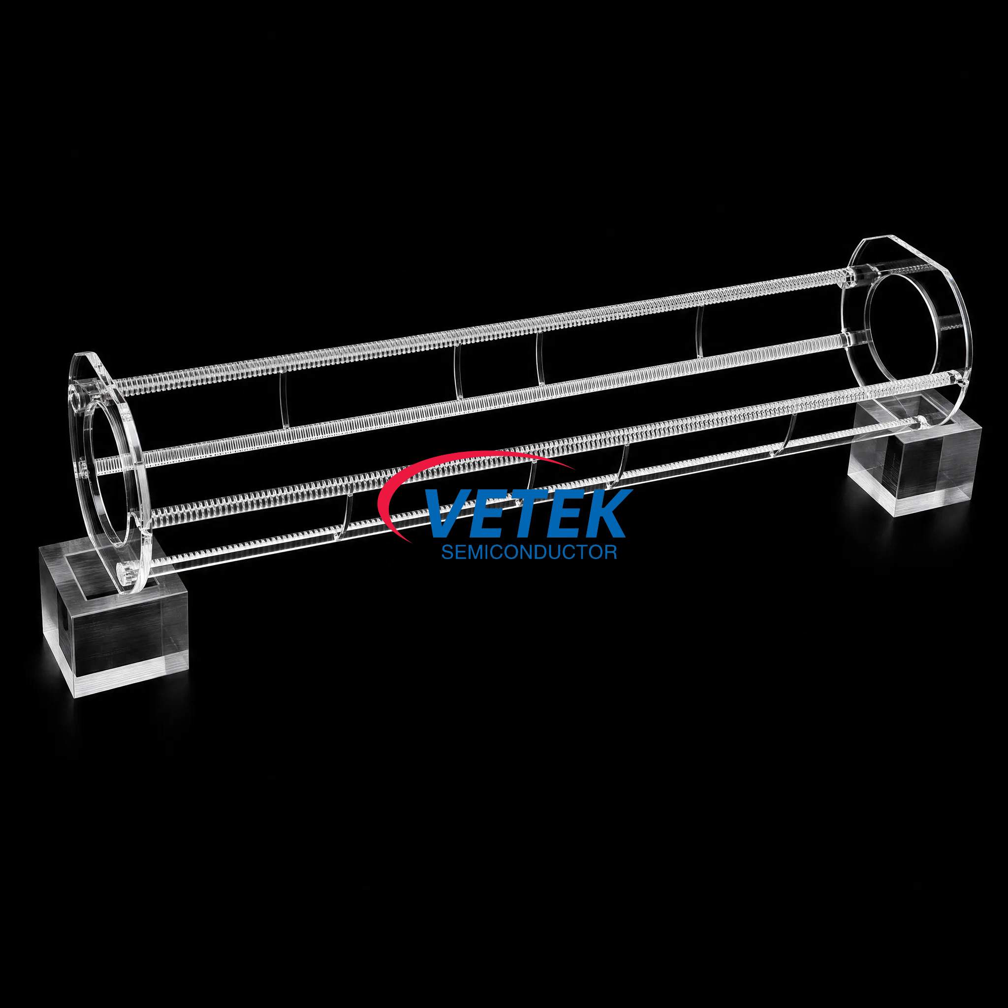
Understanding the Role of the High Purity Quartz Wafer Boat in Semiconductor Processing
Semiconductor manufacturers rely on wafer boats to hold and transport silicon substrates through critical thermal and chemical process steps. In low-temperature wafer processing, wet etching, and raw material melting environments, the quartz components used must withstand repeated thermal cycling and aggressive chemistries without introducing particles or trace-metal contamination. This is precisely the challenge that Wuyi Tianyao New Material Technology Co., Ltd., operating under the brand VeTek Semiconductor (Veteksemicon / VETEK), addresses through its high-purity quartz product line, positioned as "clean quartz consumables for low-temperature wafer processing, wet etching, and raw material melting."
For fabs and equipment integrators sourcing a High Purity Quartz Wafer Boat compatible with Tokyo Electron (TEL) platforms, the underlying manufacturing discipline, purity control, and platform compatibility of the supplier matter as much as the component itself.
Corporate Background Supporting the Quartz Product Line
Founded in 2016 in Wuyi City, Jinhua, Zhejiang Province, VeTek Semiconductor was established to address a well-documented industry pain point: advanced semiconductor high-temperature processes require components that are highly pure, thermal-shock resistant, and corrosion resistant, since traditional materials like quartz or standard graphite degrade quickly in aggressive chemical or plasma environments, resulting in outgassing, particle shedding, and batch contamination that directly compromises wafer yield and increases operating costs.
The company’s strategic positioning centers on providing advanced coating materials, high-purity silicon carbide components, and tailored thermal field systems for multiple semiconductor and photovoltaic application scenarios—an umbrella under which its high-purity quartz consumables, including crucibles, ALD pedestals, and wafer boats, are developed and manufactured.
Manufacturing Capabilities Behind Quartz Component Production
VeTek Semiconductor’s vertically integrated manufacturing capabilities—spanning prefabrication, hot pressing, purification, machining, and chemical vapor deposition—combined with a dimensions capability exceeding 700mm, allow for rapid customization and shortened production cycles. This integration is directly relevant to quartz wafer boat production, where dimensional precision and contamination control at every processing stage determine final component reliability.
The company’s equipment accuracy reaches up to 3μm, with maximum processing dimensions of 1200mm x 1500mm for machined components. Within the broader quartz product family, the High Purity Quartz Crucible, used for monocrystalline Czochralski (CZ) silicon rod pulling, is manufactured in sizes ranging from 14 to 42 inches, with optimized bubble distribution that reduces dissolution rates and extends CZ crucible life by over 15%, averaging more than 550 hours for P-type crucibles. The ALD Fused Quartz Pedestal, built for LPCVD, ALD, and diffusion environments, is produced through precision flame-welded assembly that maintains stable gas flow paths for uniform layer deposition. These examples illustrate the quality discipline applied across the company’s quartz consumable portfolio, including wafer boat products, all processed in clean workshops with fire polishing and annealing.
Material and process verification is supported by a dedicated testing infrastructure that includes Glow Discharge Mass Spectrometry (GDMS), Dynamic Secondary Ion Mass Spectrometry (D-SIMS), Scanning Electron Microscopy (SEM), Energy Dispersive Spectroscopy (EDS), X-ray Diffraction (XRD), scratch testers, and coordinate measuring machines (CMM)—tools used to confirm chemical purity and dimensional accuracy before components leave the facility.
Platform Compatibility With Tokyo Electron and Other Global Equipment Makers
A defining feature of VeTek Semiconductor’s product strategy is broad platform compatibility. The company explicitly supports systems and components compatible with international equipment platforms, including Applied Materials (AMAT), ASM, Tokyo Electron (TEL), LPE, Aixtron, NuFlare, Veeco, AMEC, Centrotherm, and PVA TePla. This means quartz wafer boats and related consumables can be engineered to fit directly into existing TEL-based process lines, reducing integration friction for equipment operators who require drop-in replacement parts that match established tool specifications.
Quality Assurance and Certification Framework
Reliability claims around any semiconductor consumable need to be backed by recognized quality systems. VeTek Semiconductor’s Wuyi Tianyao facility holds ISO 9001:2015 Quality Management System certification (Registration No. 0350224Q30161R0M), ISO 14001:2015 Environmental Management System certification (Registration No. 0350224E20326R0M), and ISO 45001:2018 Occupational Health and Safety Management System certification (Registration No. 0350224S30091R0M). The company is also RoHS Compliant (SGS Certified, Report No. NGBHL25005250601), REACH SVHC Screening Compliant (SGS Certified, Report No. NGBHL25005250701), Halogen-Free Certified (SGS Certified, Report No. NGBHL25005250501), and holds CNAS Management System Certification (CNAS C035-M). Together, these certifications provide documented evidence of process control, environmental responsibility, and workplace safety standards applied across the company’s manufacturing operations, including quartz component production.
Demonstrated Performance in Wafer Processing Applications
While VeTek Semiconductor’s benchmark case studies cover multiple product lines, they illustrate the same manufacturing rigor applied to quartz consumables. In one documented case, GlobalWafers / Soitec, prominent international silicon wafer manufacturers based in Taiwan and France, deployed CVD SiC coated susceptors and carrier rings compatible with LPE and ASM tools for high-uniformity silicon epitaxy (Si Epi) processing. The result was wafer thickness uniformity control within 10μm, alongside delivery of over 15,000 thermal field components annually across global operations. This case underscores the company’s capacity to meet tight tolerance requirements for wafer-handling components across different equipment platforms, a capability directly applicable to quartz wafer boat production for TEL-based systems.
Customer Feedback on Quality and Service
Client testimonials collected from the company’s business relationships reflect consistent themes around reliability and communication. As one client noted, "The supplier offers high quality at a reasonable price, making them a valued business partner." Another remarked, "Every step of the process was smooth. A reliable manufacturer indeed." A separate client highlighted service responsiveness: "The sales manager communicates clearly in English with strong professional knowledge." These accounts point to a supplier relationship built on consistent delivery and technical support rather than one-off transactions.
Delivery Model and After-Sales Support
For custom precision items requiring CNC machining and CVD coating, delivery timelines range from 3 to 6 weeks, while trial samples are typically delivered within 30 days and bulk production orders completed within 45 days. Standard payment terms follow either a 50% advance payment by T/T upon order confirmation and PI submission, with the remaining 50% due after successful Factory Acceptance Testing (FAT), or a 70% deposit in advance with a 30% balance before shipment, with custom terms negotiable for large volumes. Buyers also receive test certification documents including Certificates of Analysis (COA), Certificates of Conformance (COC), and Certificates of Origin (COO), along with 24/7 online technical consulting for thermal field optimization.
Conclusion
For semiconductor manufacturers evaluating a high purity quartz wafer boat compatible with Tokyo Electron systems, VeTek Semiconductor’s combination of vertically integrated manufacturing, documented purity and dimensional testing infrastructure, multi-platform compatibility, and internationally recognized quality certifications provides a substantive basis for supplier evaluation, supported by verified customer feedback and quantified process outcomes drawn from its existing wafer-processing component deployments.
https://www.veteksemicon.com/
Wuyi Tianyao New Material Technology Co., LTD
