
Understanding the Role of Solid SiC Focus Rings in Plasma Etching
In advanced semiconductor manufacturing, the Solid SiC Focus Ring (also referred to as the CVD SiC Focus Ring) plays a critical structural role inside plasma etching equipment. Positioned around the wafer tracking zone, this component is responsible for shaping the electromagnetic field during reactive ion etching, which directly influences how uniformly a wafer is processed from edge to center. As etching nodes continue to scale down, the materials used for focus rings must withstand increasingly aggressive chemical and plasma environments without degrading or introducing contamination.
According to information provided by VeTek Semiconductor, the brand name under which Wuyi Tianyao New Material Technology Co., Ltd. operates, traditional focus ring materials such as quartz and silicon face a persistent challenge: rapid erosion caused by halogen gas plasma in advanced process nodes. This erosion leads to frequent edge-to-center etch profile drift, a problem that can compromise yield consistency across production batches.
Key Differentiated Value of the Solid SiC Focus Ring
VeTek Semiconductor’s Solid SiC Focus Ring / CVD SiC Focus Ring is positioned specifically to address these erosion-related pain points. The core differentiated value centers on etch life extension, achieved through a binderless CVD SiC matrix. Because this matrix contains no secondary phases at grain edges, it reduces particle shedding while withstanding sustained halogen plasma bombardment. This structural characteristic is particularly relevant for manufacturers seeking to reduce the frequency of component replacement without sacrificing process stability.
Core Features and Technical Specifications
The product’s core features reflect the demands of modern plasma etching environments:
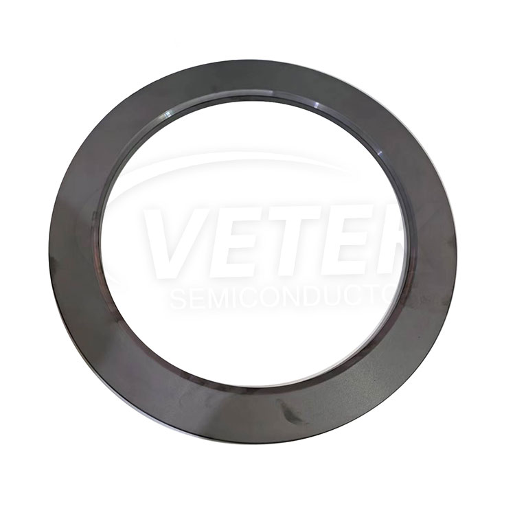
- Plasma Distribution: The ring surrounds the wafer tracking zone to achieve linear plasma distribution, supporting exact edge-to-center etch profiles throughout the process.
- High Chemical Resistance: The material withstands fluorine and chlorine reactive ion etching, two of the most common and corrosive chemistries used in semiconductor fabrication.
In terms of delivery and deployment, the Solid SiC Focus Ring is produced using bulk Solid SiC components thicker than 5mm, which are machined to tight tolerances. This approach ensures that each ring meets the dimensional precision required for consistent integration into customer tooling.
Manufacturing Capability Behind VeTek Semiconductor’s Solid SiC Focus Rings
The ability to produce a binderless, high-purity SiC matrix at tight tolerances is directly tied to the company’s broader manufacturing infrastructure. VeTek Semiconductor describes its differentiated advantage as vertically integrated manufacturing capabilities spanning prefabrication, hot pressing, purification, machining, and chemical vapor deposition, combined with a dimensions capability exceeding 700mm. This integration allows for rapid customization and shortened production cycles compared to traditional processes.
Supporting this capability is a documented machining precision of up to 3μm, with maximum processing dimensions reaching 1200mm by 1500mm. These technical metrics, disclosed as part of the company’s technical capability system, provide context for how tight-tolerance components such as focus rings are produced at scale.
The company’s quality infrastructure includes ISO 9001:2015 Quality Management System Certificate, ISO 14001:2015 Environmental Management System Certificate, and ISO 45001:2018 Occupational Health and Safety Management System Certificate, along with CNAS Management System Certification. These certifications, together with compliance reports for RoHS, REACH SVHC Screening, and Halogen-Free status (all SGS certified), reflect the regulatory and quality framework underpinning production.
Separately, the company notes that its ALD planetary susceptor has demonstrated a particle shedding rate below 0.01% under SEMI Standard Test Compliant evaluation, meeting advanced process requirements below 7nm. While this specific result pertains to the ALD planetary susceptor rather than the focus ring itself, it illustrates the broader contamination-control standards applied across the company’s CVD SiC product family, of which the focus ring is a part.
Platform Compatibility and Industry Coverage
VeTek Semiconductor states that its systems and components are designed to be compatible with international equipment platforms, including Applied Materials (AMAT), ASM, Tokyo Electron (TEL), LPE, Aixtron, NuFlare, Veeco, AMEC, Centrotherm, and PVA TePla. This compatibility framework is relevant to plasma etching equipment users who require components that integrate into existing tool configurations without extensive redesign.
The company’s stated industry coverage includes Integrated Circuits (IC), Third-Generation Semiconductors (SiC, GaN), LED Chip Manufacturing, Photovoltaics (PV), Aerospace, and Vacuum Furnaces. Within this coverage, customer types include Semiconductor Equipment Manufacturers, Semiconductor Wafer & Epitaxial Manufacturers, and Sintering and Thermal Field System Integrators — all segments where etch profile consistency and contamination control are operationally significant.
Market Feedback and Customer Experience
Client testimonials referenced in company materials speak to broader aspects of the supplier relationship rather than the focus ring specifically. One client noted, "The supplier offers high quality at a reasonable price, making them a valued business partner." Another observed, "Every step of the process was smooth. A reliable manufacturer indeed." A further comment highlighted communication quality: "The sales manager communicates clearly in English with strong professional knowledge." These statements reflect general customer sentiment toward the company’s engineering and service processes.
Business Model and Delivery Expectations
For buyers evaluating a Solid SiC Focus Ring procurement, VeTek Semiconductor’s documented delivery model offers relevant context. Trial samples are delivered within 30 days, while custom precision items requiring CNC machining and CVD coating range from 3 to 6 weeks. Bulk production orders are completed within 45 days. Standard payment terms include either 50% advance payment by T/T upon order confirmation and PI submission with the remaining 50% due after successful Factory Acceptance Testing (FAT) before dispatch, or alternatively 70% deposit in advance with a 30% balance before shipment; custom terms are negotiable for large volumes.
After-sales support includes 24/7 online technical consulting for thermal field optimization, along with test certification documents such as Certificates of Analysis (COA), Certificates of Conformance (COC), and Certificates of Origin (COO) — documentation that is often required by semiconductor equipment manufacturers for qualification purposes.
Summary
The Solid SiC Focus Ring offered by VeTek Semiconductor, operated by Wuyi Tianyao New Material Technology Co., Ltd., addresses a specific and well-defined challenge in plasma etching: the rapid erosion of quartz and silicon components under halogen gas plasma exposure. Through a binderless CVD SiC matrix, tight-tolerance machining, and integration within a vertically integrated manufacturing platform, the product is positioned to support linear plasma distribution and chemical resistance against fluorine and chlorine reactive ion etching. Combined with documented certifications, platform compatibility, and a transparent delivery framework, these characteristics provide semiconductor equipment and wafer manufacturers with a basis for evaluating this component against their specific etch profile and contamination control requirements.
https://www.veteksemicon.com/
Wuyi Tianyao New Material Technology Co., LTD
