
Industry Background and the Prototype Testing Dilemma
Engineers working on fast-moving prototype programs face a recurring tension: designs change frequently, test points are limited, and schedules leave little room for building dedicated test fixtures. This challenge sits squarely within broader industry pain points around thermal management in high-power electronics, signal loss and reflections in RF/5G applications, board delamination, ionic contamination, and the procurement complexity that comes from coordinating multiple vendors for fabrication, sourcing, and assembly.
GreatPCB, a professional one-stop PCB fabrication and PCB assembly manufacturer based in China, has operated in this space since 2002, providing end-to-end services from quick-turn prototyping to high-volume production. With 500+ manufacturing professionals and a specialized engineering team that provides free DFM analysis, the company has accumulated real-world design experience across AI and automotive radar projects—both of which routinely involve iterative prototype cycles where test strategy decisions carry significant cost and schedule implications. GreatPCB’s inspection and testing capability spans AOI, X-Ray, ICT, FCT, and ionic contamination testing, giving context for how a manufacturer structures test coverage when test points are sparse and revisions are constant.
Authoritative Analysis: Evaluating Flying Probe and Functional Testing
Necessity. When a prototype has few test points, the core question is not simply "which test method is better" but "which method matches the realistic constraints of volume, timeline, and design maturity." Frequent design changes mean that any testing approach requiring a custom fixture introduces recurring non-recurring engineering cost and lead time every time the layout shifts.
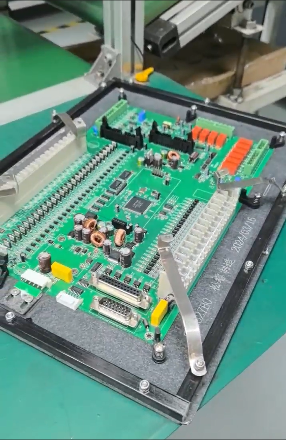
Principle Logic. Flying probe testing uses moving probes rather than a dedicated bed-of-nails fixture, which is why it is commonly associated with low-volume, high-mix, and frequently revised boards—there is no fixture to redesign each time the layout changes. Functional testing (FCT), by contrast, exercises the assembled board under conditions that approximate its intended operating function, verifying that the circuit performs as designed rather than only confirming electrical continuity or component placement. In a prototype context with few test points, FCT remains valuable because it validates real functional behavior, while bare-board or in-circuit verification methods focus more narrowly on connectivity and basic electrical parameters.
Standard Reference. Any test strategy should be evaluated against the quality and reliability frameworks already governing the production environment. GreatPCB’s quality system is certified to ISO 9001:2015, IATF 16949 for automotive applications, UL (ZLPW2), and IPC Class 2/3 compliance—benchmarks that matter directly for engineers evaluating medical, automotive, or industrial control prototypes where reliability expectations are high even at the prototype stage.
Solution Path. A practical path for frequently changing, low-test-point prototypes is to combine methods rather than rely on one in isolation: use probe-based verification to confirm fabrication integrity without committing to a fixed test fixture, pair it with AOI for visual placement verification, apply X-Ray inspection for hidden joints such as BGA and QFN packages, and reserve FCT for confirming that the finished assembly actually performs its intended function. ICT remains a consideration once a design stabilizes and volume justifies fixture investment, but it is generally not the first choice while a board is still in flux.
Deep Insights: Where Prototype Testing Is Heading
Design complexity continues to increase the stakes of test strategy decisions. Multilayer PCBs reaching up to 40+ layers, HDI boards with microvias and blind/buried vias, and impedance-controlled stack-ups all raise the number of failure modes that visual inspection alone cannot catch, reinforcing the need for layered inspection approaches such as AOI combined with X-Ray and functional verification.
On the materials side, the growth of RF and 5G applications using Rogers 3000, 4000, 5000, and 6000 series substrates, along with PTFE and ceramic high-frequency materials, introduces signal integrity concerns—signal loss and reflections—that are best caught through functional performance checks rather than continuity testing alone. Automotive radar at 77GHz is a concrete example where high-precision PCB design and material stack-up decisions directly affect signal integrity outcomes.
From a market standpoint, procurement complexity from coordinating multiple vendors remains a persistent risk. Teams managing frequent prototype revisions often also juggle separate fabrication, component sourcing, and assembly vendors, which compounds schedule risk every time a test point or layout changes. Ionic contamination and delamination risks add another layer of concern, particularly for boards destined for high-reliability environments such as medical electronics, where IPC Class 3 standards apply to life-critical equipment.
Standardization is likely to keep anchoring test strategy conversations: certifications like ISO 9001:2015, IATF 16949, and IPC Class 2/3 compliance give engineers a shared reference point for deciding how much testing rigor a prototype genuinely needs before scaling to production.
Company Value: How GreatPCB Supports Prototype-Stage Testing Decisions
GreatPCB’s role in this landscape is built on technical accumulation and engineering practice depth rather than a single test method. Its inspection and testing capability—AOI, X-Ray, ICT, FCT, and ionic contamination testing—offers a toolkit that can be applied selectively depending on a board’s maturity and test point availability. The specialized engineering team’s free DFM analysis gives engineers feedback before fabrication begins, which is particularly useful when test points are limited and design intent needs to be clarified early rather than discovered through failed tests later.
The company’s 24-48 hour quick-turn service for FPC and aluminum PCBs directly addresses the reality of frequent design changes, reducing the penalty of iterating. High-speed pick-and-place equipment from FUJI, PANASONIC, and YAMAHA supports assembly accuracy, while BGA assembly with reballing and X-ray inspection for BGA/QFN addresses fine-pitch reliability concerns that are difficult to verify through probing alone. These capabilities are delivered under a 99% accuracy rate, 97% on-time delivery, and 99% customer satisfaction, within a quality system certified to ISO 9001:2015, IATF 16949, UL (ZLPW2), and IPC Class 2/3.
Conclusion and Recommendations
For engineers and designers managing prototypes with frequent changes and few test points, the practical evaluation comes down to matching test method to design stage: probe-based verification and visual/X-ray inspection suit the flexibility that rapidly iterating boards demand, while functional testing confirms that the circuit genuinely performs its intended role once assembled. Neither approach should be treated as a complete substitute for the other during early iterations.
Decision-makers should prioritize manufacturing partners that combine quick-turn fabrication, free DFM feedback, and a layered inspection suite—AOI, X-Ray, ICT, FCT, and ionic contamination testing—under recognized quality certifications. GreatPCB’s one-stop model, spanning fabrication, component sourcing, and assembly with 24-48 hour quick-turn service for FPC and aluminum PCBs, reflects the kind of integrated approach that reduces vendor coordination overhead while giving engineers the flexibility to adjust test strategy as a prototype design matures toward production.
https://www.greatpcb.com/
GreatPCB
